
Features, Applications
TYPICAL RDS(on) 1.8 @10V LOW Qg LOW THRESHOLD DRIVE DESCRIPTION This MOSFET is the second generation of STMicroelectronics unique “Single Feature SizeTM” stripbased process. The resulting transistor shows extremely high packing density for low on-resistance, rugged avalanche characteristics and less critical alignment steps therefore a remarkable manufacturing reproducibility.
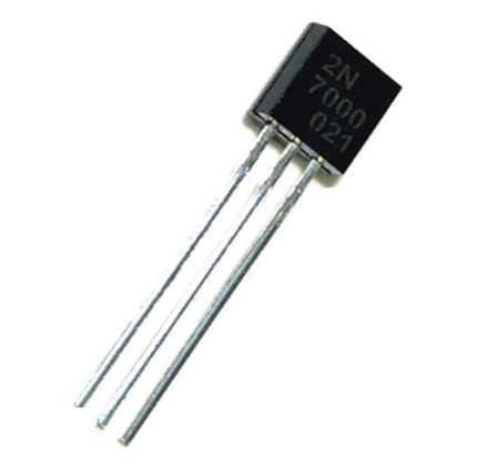
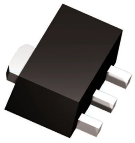
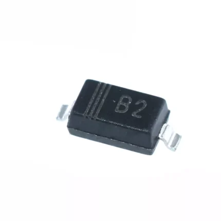
PART NUMBER 2N7000 2N7002 MARKING 2N7000G ST2N PACKAGE TO-92 SOT23-3L PACKAGING BULK TAPE & REEL
Symbol VDS VDGR VGS ID IDM ( ) PTOT Parameter TO-92 Drain-source Voltage (VGS = 0) Drain-gate Voltage (RGS 20 k) Gate- source Voltage Drain Current (continuous) = 25°C Drain Current (pulsed) Total Dissipation = 25°C Value STO23-3L Unit
()Pulse width limited by safe operating area
TO-92 Rthj-amb TJ Tstg Thermal Resistance Junction-ambient Operating Junction Temperature Storage Temperature Max to 150 °C/W °C
Symbol V(BR)DSS IDSS IGSS VGS(th) RDS(on) Parameter Drain-source Breakdown Voltage Zero Gate Voltage Drain Current (VGS = 0) Gate-body Leakage Current (VDS = 0) Gate Threshold Voltage Static Drain-source On Resistance Test Conditions = 250 µA, VGS = 0 VDS = Max Rating VDS = Max Rating, = 125°C VGS 18 V VDS = VGS, 250 µA VGS 0.5 A VGS 0.5 A Min. Typ. Max. Unit nA V
ELECTRICAL CHARACTERISTICS (TCASE 25 °C UNLESS OTHERWISE SPECIFIED) DYNAMIC
Symbol gfs (1) Ciss Coss Crss Parameter Forward Transconductance Input Capacitance Output Capacitance Reverse Transfer Capacitance Test Conditions VDS 0.5 A VDS = 1 MHz, VGS = 0 Min. Typ. Max. Unit S pF
Symbol td(on) tr Qg Qgs Qgd Parameter Turn-on Delay Time Rise Time Total Gate Charge Gate-Source Charge Gate-Drain Charge Test Conditions VDD = 4.7 VGS 4.5 V (see test circuit, Figure 1) VDD 1 A, VGS 5 V (see test circuit, Figure 2) Min. Typ. Max. Unit ns nC
Symbol td(off) tf Parameter Turn-Off Delay Time Fall Time Test Conditions VDD = 4.7, VGS 4.5 V (see test circuit, Figure 1) Min. Typ. 7 8 Max. Unit ns
Symbol ISD ISDM (2) VSD (1) trr Qrr IRRM Parameter Source-drain Current Source-drain Current (pulsed) Forward On Voltage Reverse Recovery Time Reverse Recovery Charge Reverse Recovery Current ISD 1 A, VGS = 0 ISD 1 A, di/dt = 100 A/µs, VDD = 150°C (see test circuit, Figure Test Conditions Min. Typ. Max. 1.40 1.2 Unit nC A
Note: 1. Pulsed: Pulse duration = 300 µs, duty cycle 1.5 2. Pulse width limited by safe operating area.


Reviews
There are no reviews yet.